Sensors & Transmitters
Changzhou Boyan Optical Co., Ltd
26 Dec 2025
(
)
Get Your Quote Now : US$ 20/ Piece
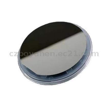
| Production Method | CZ |
| Diameter | 2inch / 3inch / 4inch/ 6inch / 8 inch |
| Thickness | 100um,200um,300um,400um,500um,600um,700um,800um,900um,1000um |
| Type | N type / P type |
| Orientation | <111> , <100>,<110> |
| Resistivity | 0.002~25000 Ω.cm |
| Flatness TIR | <3um |
| Warping degree TTV | <10um |
| Flexibility BOW | <10um |
| Roughness | <0.5nm |
| Granularity | 10 ( for size >0.3um) |
| Application | Used for synchrotron radiation sample carrier, PVD/CVD coating as substrate, magnetron sputtering growth sample, XRD, SEM, Atomic force, infrared spectroscopy, fluorescence spectroscopy and other analysis test substrates, molecular beam epitaxial growth substrates, X-ray analysis of crystalline semiconductors |
Our premium Monocrystalline Silicon Wafer offers unmatched cost performance. Despite its superior quality and advanced features, it is competitively priced to ensure maximum value for our customers. Invest in our product and experience significant cost savings in your semiconductor manufacturing processes. --- Experience the difference our premium Monocrystalline Silicon Wafer can make in your semiconductor manufacturing operations. With its exceptional conductivity, accuracy, and efficiency-enhancing features, this product is the perfect choice for semiconductor manufacturers, research institutions, and technology companies. Upgrade your production processes with our top-tier product today.Monocrystalline Silicon Wafers are highly pure silicon wafers that are composed of a single crystal structure, making them highly efficient for a wide range of applications in the semiconductor and electronics industries. These wafers are known for their superior quality and performance compared to other types of silicon wafers.The type of Monocrystalline Silicon Wafer is determined by the crystalline orientation of the silicon atoms in the wafer. Different types of Monocrystalline Silicon Wafers include (100) and (111) orientations, which offer different properties and characteristics. The (100) orientation is widely used in the semiconductor industry due to its high electron mobility, while the (111) orientation is preferred for certain applications that require high crystal symmetry.Monocrystalline Silicon Wafers are available in different resistivity levels, ranging from low resistivity to high resistivity. The resistivity of the wafer plays a crucial role in determining the electrical properties of the semiconductor devices manufactured on it. Low resistivity wafers are suitable for power devices, while high resistivity wafers are used for integrated circuits and other microelectronic applications.Flatness is another important parameter that defines the quality of Monocrystalline Silicon Wafers. The flatness of the wafer refers to how smooth and uniform the surface of the wafer is. High flatness wafers are essential for ensuring the accuracy and reliability of the semiconductor devices fabricated on them. Monocrystalline Silicon Wafers with high flatness are preferred for applications that require precise patterning and etching processes.Monocrystalline Silicon Wafers find wide applications in the semiconductor industry, including the fabrication of integrated circuits, sensors, solar cells, and MEMS devices. These wafers are also used in research and development activities for studying the properties of semiconductor materials and devices. The high purity and crystal quality of Monocrystalline Silicon Wafers make them ideal for demanding applications that require precise control of electrical and optical properties.The diameter of Monocrystalline Silicon Wafers is an essential parameter that determines the size of the semiconductor devices that can be fabricated on them. These wafers are available in various diameters, with common sizes ranging from 2 inches to 12 inches. Wafers with larger diameters are preferred for high-volume production of semiconductor devices, while smaller diameter wafers are used for research and prototyping purposes.In conclusion, Monocrystalline Silicon Wafers are essential materials for the semiconductor industry, offering superior quality, performance, and reliability. These wafers are available in different types, resistivity levels, flatness specifications, and diameters to meet the diverse requirements of modern semiconductor applications. With their excellent properties and versatility, Monocrystalline Silicon Wafers play a critical role in advancing technology and innovation in the electronics industry.










Clients Reviews